Atomic force microscopy
Atomic Force Microscopy (AFM) is a high-resolution imaging technique used to analyze the surface topography and material properties with a sub-nanometer resolution. The technique allows studying various material properties such as the surface roughness, topological features, surface defects as well as mechanical and electromagnetic properties of the material, and is ideal for analyzing thin films, nanoparticles and organic materials.

Some of our AFM services
AFM surface roughness measurement
AFM surface imaging
Prices excluding VAT.
- Fast turnaround times
- Personal service from method experts
- Competitive prices
- Result accuracy guarantee
What is AFM analysis used for?
AFM is a widely used characterization technique that provides high-resolution, three-dimensional mapping of the sample surface with a sub-nanometer resolution. This makes AFM ideal for analyzing nanoscale features such as surface roughness, topological features, and surface defects. In addition to topography, AFM can also map local mechanical and electromagnetic properties such as stiffness, adhesion, conductivity, surface potential, and magnetic domains through specialized modes.
AFM is suitable for a wide range of materials, including semiconductors, thin films, nanomaterials, metals, polymers, and biological samples. It is particularly valuable for characterizing thin films deposited by techniques such as Chemical Vapor Deposition (CVD), Atomic Layer Deposition (ALD), Physical Vapor Deposition (PVD), and spin coating. Unlike many other surface analysis techniques, AFM does not require a vacuum or conductive samples. It can also operate in air, vacuum, or liquids, allowing for analysis of a wide range of materials.
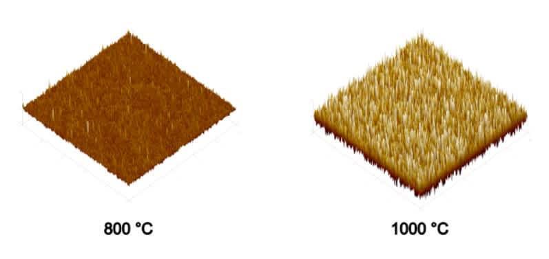
As an example, AFM allows us to analyze the surface roughness of thin films processed at different temperatures. Quantitative data, such as root mean square (RMS) roughness or feature height distribution, can be extracted from the resulting 2D and 3D surface maps.


While AFM is a highly versatile and precise tool, its capabilities are limited by the imaging conditions. AFM can image features with a maximum height of 20 µm and areas up to 100 × 100 µm. For larger features or larger areas, we recommend using profilometry. AFM analysis is also most accurate on clean and flat surfaces, making very rough or oddly shaped surfaces difficult to analyze. However, when properly optimized, AFM provides invaluable data on surface properties essential in product development, quality control, and process optimization.
Measurlabs frequently provides AFM measurements for several large clients in the semiconductor industry. One of these is Okmetic, the world's seventh largest silicon wafer manufacturer. Read more about our cooperation here:
How does atomic force microscopy work?
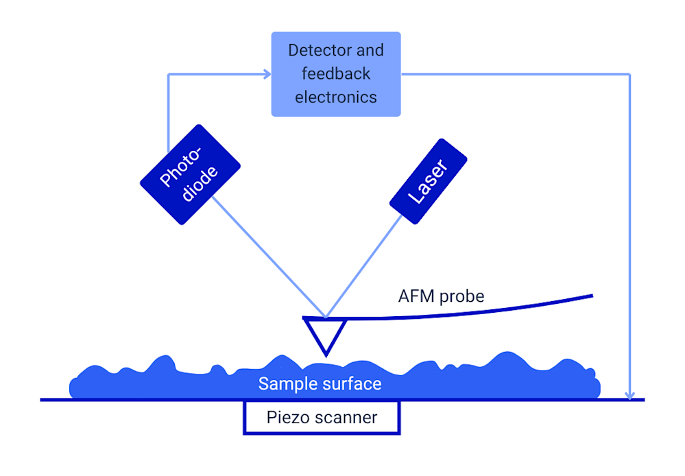
AFM operates by scanning a sharp tip mounted on a flexible cantilever across the sample’s surface. As the probe scans the sample surface, interactions between the tip and sample cause the cantilever to bend. A laser beam is reflected off the cantilever, tracking these deflections with high precision and recording changes in the tip's position. The recorded laser deflections are used to reconstruct a map of the sample surface.

AFM modes
AFM can operate in three different modes: Contact Mode, Tapping Mode, and Non-Contact Mode. Each mode offers its own advantages and is suited to different types of samples and measurements.
Contact mode: the tip remains in continuous contact with the sample surface during scanning. Contact mode offers high resolution and fast imaging, but applies a constant force to the sample, which can damage the sample surface. It is best suited for hard, smooth surfaces such as wafers or thin films.
Tapping mode: this is one of the most commonly used modes. In tapping mode, the cantilever oscillates so that the tip briefly touches the surface at each cycle. This reduces the pressure that can damage soft or loosely bound surfaces, while still maintaining high resolution. Tapping mode is ideal for a wide range of materials, including polymers, composites, and biological samples.
Non-contact mode: the cantilever oscillates just above the sample surface without making physical contact. The tip senses long-range attractive forces (van der Waals), which slightly alter the oscillation amplitude and frequency. This mode is very gentle and is especially useful for soft, fragile, or contamination-sensitive surfaces. However, it typically provides lower resolution than tapping or contact mode and is more sensitive to environmental noise and contamination.
Need AFM analyses?
Measurlabs offers laboratory testing with AFM for thin films and other coatings. Our testing experts are happy to help select suitable methods and make sure you get insightful results - we offer a full set of advanced techniques for analyzing thin films and semiconductors so you can get the full scope easily from one partner. We can process even large sample batches efficiently and offer quick turnaround times to allow your projects to move forward with the pace you need. Contact us through the form below to get started!
Suitable sample matrices
- Bare wafers, such as silicon (Si), silicon oxide (SiO2), silicon carbide (SiC), gallium nitride (GaN), gallium arsenide (GaAs), and Indium phosphide (InP)
- PVD, CVD, and ALD thin films
- Nanostructured surfaces
- Nanoparticles
- Polymers and organic materials
- Metals and alloys
Ideal uses of AFM
- High-resolution surface topography imaging
- Quantitative surface roughness and thickness step measurements
- Characterization of nanostructures, grains, and surface defects
- Mapping mechanical properties such as stiffness, adhesion, and elasticity
- Quality control and comparative analysis of thin film surfaces
Ask for an offer
Fill in the form, and we'll reply in one business day.
Have questions or need help? Email us at info@measurlabs.com or call our sales team.
Frequently asked questions
Measurlabs offers a variety of laboratory analyses for product developers and quality managers. We perform some of the analyses in our own lab, but mostly we outsource them to carefully selected partner laboratories. This way we can send each sample to the lab that is best suited for the purpose, and offer high-quality analyses with more than a thousand different methods to our clients.
When you contact us through our contact form or by email, one of our specialists will take ownership of your case and answer your query. You get an offer with all the necessary details about the analysis, and can send your samples to the indicated address. We will then take care of sending your samples to the correct laboratories and write a clear report on the results for you.
Samples are usually delivered to our laboratory via courier. Contact us for further details before sending samples.